A New 8051 Microcontroller: 00 - Overview & Address Unit
Introduction
One of my projects lately has been the creation of a new 8051 microcontroller using an FPGA. I decided to do this because I got tired of writing libraries to accomplish what should really be done in hardware. I am also relatively new to FPGAs, having shunned them for many years as a programmer's way of trying to hack it as an electrical engineer. I may be correct in some cases, but FPGAs are a very useful tool overall, whether you are a hobbyist, programmer, or EE. Designing a new 8051 is a way to become more acquainted with the FPGA design process. Finally, I needed an 8051 variant with protected mode and memory management features.
So, the process of creating this 8051 variant is what I will be documenting and sharing here. As always, I will not be sharing any files - if one wants to follow along at home, they will have to do the footwork themselves, learning the hardware as they do. I will not be using VHDL or similar tools, instead relying on schematic capture. The former may be better, but my mind works much better with the latter.
Also, if you are the type, for example, who frequents Stack Exchange and prefers to give your $0.02 vice simply answering some poor soul's question...move along because I am not interested in comments like "why don't you just use [insert ARM product here]", "like ZOMG jeez why are you using an 8-bit MCU this is, like, 2017" and similar things. However, I am all ears if you have good advice, suggestions, and so on. A basic familiarity with 8051 architecture is also a must.
Anyway, let's get started!
Architectural Overview
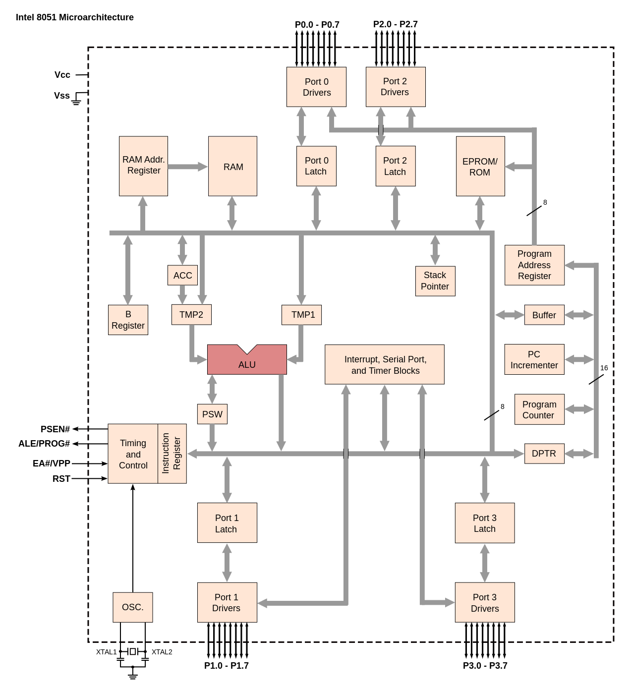
The 8051 is an architecture that is older than me; however, it remains popular today for many reasons. Figure 1 shows the architecture of the basic 8051.

Figure 1. Intel 8051 architecture. From Wikipedia
This design will not worry too much about the ports, timers, and other peripherals until the MCU core is complete. The core consists of working registers (A and B), four register banks of eight registers each, 256 addressable bits, an address unit (PC, SP, DPTR), an ALU, and interrupt system. In this post we will be focusing on the address unit.
Address Unit
Base Address
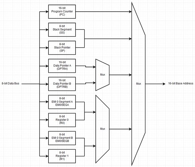
Addressing operations in almost all 8051 variants are simple and straightforward - a base address is formed by the PC, DPTR, SP, Ri (R0 or R1), or direct address. The PC and DPTR form 16-bit addresses, while the SP, Ri, and direct addresses are only 8-bits. This design will extend 8-bit addresses to 16-bits through the use of two register types - Stack Segment (SS) and External Memory Interface (EMI) registers. When enabled, the SS is used as the most significant byte (MSB) of a 16-bit address. This allows the stack to be placed in external RAM (XRAM) vice being limited to the 256 byte internal RAM (IRAM). This also allows, if the programmer so chooses, to manage stacks for different processes using the SS register as a selector. Likewise, the EMI register is used as the address MSB during accesses using Ri or direct addressing. Figure 2 shows all registers involved in generating a base address.

Figure 2. Base address block diagram
The original, as well as many new 8051s have a single data pointer (DPTR) that can be used for both code and data memory accesses. Other 8051 variants have dual DPTR configuration, where the active DPTR is selected using a bit in a control register. This design follows the latter, using two DPTRs and associated control bits.
Various control registers allow the programmer to select which base register is used for MOVC and MOVX instructions involving the DPTR. The programmer may select the PC, SS:SP, or DPTR (A or B), which will then be automatically used when the respective MOVC and MOVX instructions are executed. Upon power-on or hard reset, DPTRA is selected as the base address to maintain compatibility with existing 8051 software. The PC is always used for instruction fetches, while the SS:SP is always used for instructions accessing the stack.
PC (16)
SS:SP (8:8)
DPTRA (16)
DPTRB (16)
EMI0ADRA:R0 (8:8)
EMI0ADRB:R1 (8:8)
Direct Address (8)
These registers, and register pairs, comprise the address unit's base address section. In addition to the base address, the address unit contains index, scale, and offset registers used to form a "final index" that can be added to the base address. This provides hardware support for implementing table structures used in operating systems, buffers, sorting algorithms, and more.
Index and Scale Registers
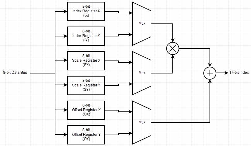
Most 8051 variants do not have a hardware method to implement indexing. This design will include hardware support for indexing - the Index X (IX) and Index Y (IY) registers. Also included are scaling registers, Scale X (SX) and Scale Y( SY). The scaling registers allow the value in an index register to be scaled by an arbitrary value. Index registers and scale registers assist the programmer in easily traversing and managing various table structures. An effective index, or the final value of a combined index and scale register, is equal to the value in the index register multiplied by the value in the scale register. Index and scale operations are controlled by their respective control registers, and can be independently enabled to support various operations.
Offset Registers
Along with the indexing system, the ability to add an offset to an effective index expands the capabilities of this 8051's address unit. Two offset registers are included, Offset X (OX) and Offset Y (OY). The offset registers allow table structures to easily be stepped through.

Figure 3. Index, scale, and offset register block diagram
Base Address and Index Register Pairing
Each DPTR is permanently paired with its own index, scale and offset registers. DPTRA is associated with the IX, SX, and OX registers, while DPTRB is associated with the IY, SY, and OY registers.
Logical Address Calculation
The address unit forms logical addresses, which may then be used directly as physical addresses, or fed to a memory management unit for further translation. Logical addresses (LA) for memory accesses using MOVC and MOVX are calculated using the following formula:
When performing instruction fetches or stack operations, the LA is simply equal to the base address.
Auto-Increment and Decrement
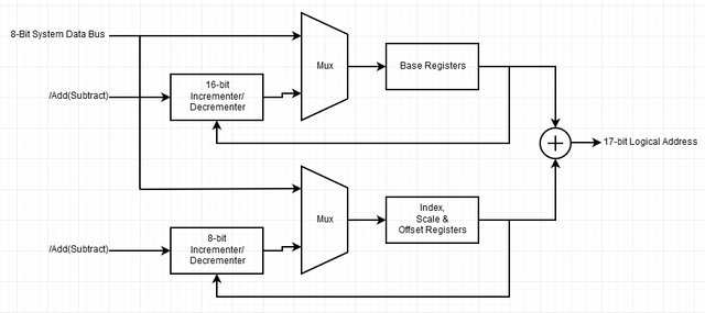
All registers except the scale registers can be set to auto-increment or decrement after each memory access. The PC is set to always auto-increment with each instruction fetch; however, the value of the PC does not change when it is used to access memory with MOVC and MOVX instructions.
By default, the SP is incremented with each stack operation, the SS only being incremented or decremented when it is enabled for stack accesses. The SS:SP may be set to auto-decrement with each stack access.

Figure 4. Complete address unit sans control and configuration registers
Auto-Swap
To make copying and other operations more efficient, the address unit can be set to automatically alternate the active base address and index registers. The ability to use one base/index register set for reads and the other for writes is also available.
Control and Configuration
The operation of each of these registers is controlled by its respective control register. Generally each base, index, and offset register contains the following configuration options:
Auto Increment/Decrement Enable
Increment/Decrement Select
Read/Write Only Enable
Read/Write Only Select
Closing Thoughts
The material presented here is merely the basic concept for the 8051 address unit being designed. As the design is implemented, additional control and other circuitry will likely be needed. The next post on this subject will include schematics of the finalized address unit, after which I will move on to other components of the microcontroller core.
Upvotes are the way I know people here on Steemit want to see more content like this, so if you liked this post and/or project, please click the upvote button! If people do not find this content interesting, there is no point in spending the time to put it here.
If you really liked it, I am always happy to find couch Satoshi under the cushions!

1CgzHKrPQrho5yMp8iUKWRDdpG8V7AuRgA
wonderfull ......thank you so much................