AREAS OF APPLICATIONS OF SEMICONDUCTOR P-N JUNCTION DIODE
In my previous articles, I was able to go deeply into the basis of semiconductors ranging from their basic operations to how they are biased. Today, I shall draw the curtain on semiconductors by exploring through their applications in the field of electronics. Did you miss the previous articles, feel free to check them out here:
Link 1
Link 2
APPLICATIONS OF P-N JNCTION DIODE
P-N junction diode as a semiconductor has areas of applications among which are the following:
P-N JNCTION DIODE AS A SWITCH:
An ideal electronic switch alternates between two states of operations. These are FULLY ON and FULLY OFF states. FULLY ON is the state of zero voltage (zero potential drop) and zero impedance (resistor). Recall from Ohms Law, V=IR. Then if V=0, R=0 as well. FULLY OFF on the other hand is the state of zero current flow and infinite impedance.
The forward bias operation of the diode represents the FULLY ON condition. However, when diodes are in their reverse bias mode, they are said to be used as a FULLY OFF switches.
But unlike an ideal switch, a conducting diode has a small forward voltage drop across its junction, the magnitude of which depends on the junction temperature, manufacturing technique and the type of materials (elements) used in making the PN junction device.
P-N JUNCTION AS A VARIABLE CAPACITOR (VARACTOR):
The width of the depletion region of a P-N junction (under reverse bias condition) increases as the reverse bias voltage increases. Under this condition, P-N junction behaves as a variable capacitor that is dependent on the reverse bias voltage. P terminal serves as a capacitor plate, N terminal performs the functions of the other plates, and the depletion region in this case represents the dielectric material between the two parallel plates of the capacitor.This capacitance is given by C= (ε°εA)/d
Where ε = relative permittivity of the semiconductor
ε°= permittivity of free space
A = Area of the junction normal to current flow
d = width of the depletion region.
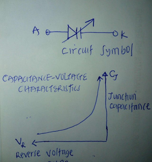
The effective width of the depletion region is a function of the magnitude of the reverse bias voltage. The lower the distance (depletion region), the lower the reverse bias voltage, the higher the junction capacitance and vice versa.
VARACTORS are classified into two namely: graded junction and abrupt junction varactors.
- GRADED JUNTION VARACTOR: This is a type of VARACTORS that has the impurity concentrations changing gradually at the P-N junction from the acceptors to the donor atoms. The junction capacitance in this case is given by: C = KV-¹/².
Where V = the reverse bias voltage given, K= diode constant.
- ABRUPT JUNCTION VARACTOR: This is a type of VARACTORS that has the impurity concentrations changing immediately (abruptly) at the P-N junction from the acceptors to the donor atoms. The junction capacitance in this case is given by: C = KV-¹/³
The circuit symbol and capacitance-voltage characteristics for a VARACTOR is shown below.
Source: @thestronics
From the curve shown above, the higher the voltage, the lower the junction capacitance and vice versa.
P-N JUNCTION AS A VOLTAGE REGULATOR (ZENER DIODE):
When a P-N junction is reverse biased, a small reverse saturation current flows in the reverse direction. This flow of current is as a result of the recombination of the minority carriers at the P-N junction. The magnitude of this current increases as the reverse bias voltage is increased. This continues like that until a particular voltage known as the breakdown voltage is reached.
At this point, there will be sudden flow of large amount of current, and this is due to the acceleration of the thermally generated electrons by electric field in a bid to produce more electron-hole pairs as they collide with the neutral toms in the depletion layer. The newly liberated electrons are also accelerated by the field to a high energy state which results into further generation of charge carriers by collision. At this stage, Avalanche breakdown sets in. The cumulative process of ionization by collision is called Avalanche Multiplication.
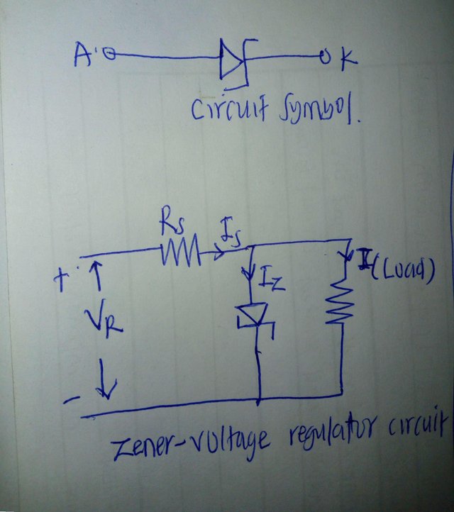
Typical application of a zener diode is the provision of a constant output voltage even though the unstabilised supply voltage varies from a wide range of values. The circuit symbol and arrangement of a zener diode is shown In the figure below.
Source: @thestronics
The reverse biased zener diode is connected in parallel across the load to ensure that relatively constant output Voltage Vs is supplied across the load. The output voltage remains relatively constant provided that the input voltage is greater than the zener diode Vz.
By Kirchhoff’s Laws:
Vs = IsRs + Vz
Is = Iz + I(load)
Rs = (Vs-Vz)/ [Iz + I(load).]
P-N JUNCTION AS A RECTIFIER:
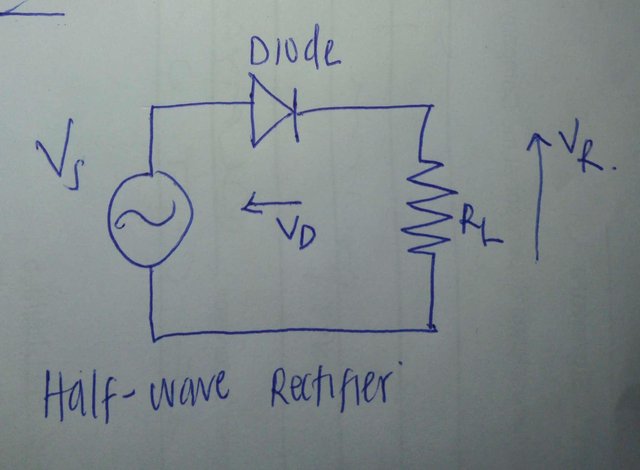
In its simplest term , rectification is the process of conversion of an alternating current (AC) signals into a Direct Current (DC) signal through the use of the device known as rectifier. The simplest rectifier is the half-wave rectifier consisting of an AC source, a diode and a resistive load connected in series as shown below.
Source : @thestronics
During the positive half cycles , the diode linking the AC source with the load is forward biased and there exists maximum flow of current from the Ac source to the load. However, during the negative half-cycle, the diode operates in its reverse bias mode and simply, no current flows from the AC source to the load.
The output of a rectifier circuit is a pulsating Direct Current (DC) signal comprising both DC and a few AC components, otherwise called ripples. These ripples are undesirable since they account for the pulsations in the output. The ratio of the root-mean-square values of the AC components to that of DC components in the rectifier output is called Ripple Factor and is given by:
Ripple Factor = V(ac)/ V(dc).
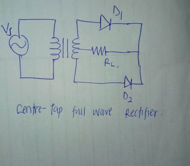
Aside the half-wave rectifier, we also have a full- wave rectifier. And unlike the half-wave that has one diode, full wave rectifier has at least two diodes. This is to ensure that current flows from the AC source to the connected Load in both the negative and the positive half-cycles.
The circit arrangement is shown below:
Source: @thestronics
In the positive half cycle, diode D1 is forward biased, D2 is reverse biased and current flows from the source to the load through the diode D1. In the negative half cycle, D2 is forward biased, D1 is reversed biased and current flows from the Ac source to the load through the diode D2.
P-N JUNCTION AS A LIGHT SOURCE AND LIGHT DETECTOR:
PN junction principles are used in the production of the popular light source, which are electronic devices that generates light as a result of the recombination of charges. Examples are Light Emitting Diode, Infrared Light Emitting Diode, and Light Amplification by Stimulation Emission of Radiation (LASER) etc.
Aside this, they are also used in the production of
Light Detectors, which are electronic devices that takes in light for the recombination of charges.
SEMIOCONDUCTORS IN THE MANUFACTURE OF MICROCONTROLLERS:
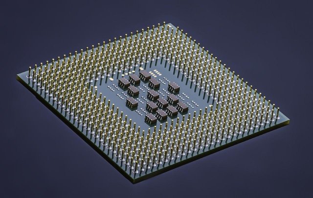
The use of semiconductors in the production of controllers constitutes their greatest applications. Microcontrollers are used widely in embedded systems design, in automation, in artificial intelligence and in robotics.
THANKS FOR TAKING YOUR TIME TO READ!!!
REFERENCES

Being A SteemStem Member
Nice post, and great information.
I have a couple points on the zener regulator circuit. You stated that, "The reverse biased zener diode is connected in parallel across the load to ensure that relatively constant output Voltage Vs is supplied across the load." I consider the output voltage Vz rather than Vs. I always consider Vs the source or supply, and Vz is the zener voltage, but that is just a label.
At any rate, while input voltage is a factor as you mentioned, regulation depends on the load current versus source current as shown in the equation. Is = Iz + I(load) The load resistor removes current from the zener diode, and the zener is considered regulated if zener current is above Izk (zener knee current). In other words if there is too much load current, the zener falls out of regulation.
The worst case as far as power dissipation for the diode is when the load is removed, or no load, as all of the current flows through the zener. Care must be taken if the load is removed that the zener can withstand Iz(max).
Again great topic, and I enjoyed the post! --3D