Electrodeposition and Characterization of CdIn2Se4 Semiconductor
Continuing with the contribution of electrochemistry to the synthesis of semiconductor materials, I bring you a summary of the most outstanding aspects of one of the articles published in my doctoral thesis, showing that electrochemically you can obtain materials with adequate structural and morphological characteristics. to be used in energetic applications..
ABSTRACT
INTRODUCTION
The semiconductor CdIn2Se4 is considered to be of technological importance because of its applications in optoelectronics and solar cells. Several physical and chemical synthetic methods have shown to be suitable for its preparation and good results are reported in the literature by using different techniques including spray-deposited thin films, chemical solution, melting and annealing techniques, thermal evaporation, vacuum evaporation, sol-gel method, epitaxial molecular beam, and others. Electrochemical techniques are now being exploited because of their potentiality and economy when used for these syntheses. In particular, CdIn2Se4 was prepared by the simple and inexpensive electrode position technique , either by sequential electrode position of individual elemental layers or by direct alloy electrode position, which provides all constituents from the same electrolytic medium in a single step. Annealing and recrystallization have also been carried out to induce reactions between the constituents. The authors of that work concluded that a sequential electrode position study allowed the optimization of both deposition potentials and solution compositions for each of the deposited elements in order to obtain better morphologies; some secondary phases were also detected. More recently, electrochemically deposited photoactive CdIn2Se4 was successfully prepared, and some other studies on electrochemically synthesized CdIn2Se4 have also been published. The aim of this work is to propose an inexpensive and simple procedure for preparing highly pure materials (particularly those of great interest for inclusion in solar cells) by electrochemical synthetic methods, as well as to characterize and study the properties of electrodeposited CdIn2Se4 films.
EXPERIMENTAL
The deposition of the films was performed by applying a double pulse potential (with an amplitude of -0.95 V, applied during 25 min, and a reverse potential of -0.50 V, applied for 6 min) at 80 °C. An additional heating treatment at 450 °C (under selenium atmosphere for 3h) was then required to obtain the ternary compound. All the electrochemical experiments were performed using a PAR 273A potentiostat / galvanostat coupled to a microcomputer. A Hitachi S-2500 scanning electron microscope coupled to an X-ray dispersive energy detector allowed us to characterize the morphology, crosssection, and elemental composition of the thin films. The crystal structure was determined using a Siemens D5005 model X-ray diffract meter. The band gap of the CdIn2Se4 thin film deposited on an ITO substrate was calculated by absorbance measurements performed on an automated Cary 17 spectrophotometer. Electrochemical impedance spectroscopy (EIS) experiments were performed using an AUT 302N potentiostat / galvanostat coupled to a FRA 32 M 110 impedance module.
RESULTS
Electrodeposition
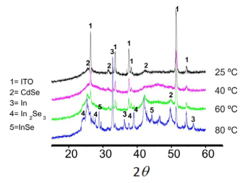
A systematic study of the electrodeposited binary phases as a function of the solution temperature was carried out using 5.0 mM SeO2, 5.0 mM CdCl2.H2O, and 1.0 mM In (III) in 0.5 M Na2SO4 at pH 2.5. Pourbaix diagrams were additionally considered to find the appropriate experimental conditions for preparing the binary semiconductor phases. A double-potential pulse method (-0.95 V for 25 min and -0.50 V for 6 min) on titanium and ITO supports was applied at 80°C, chosen after evaluating the system. Figure 1 shows diffract grams of the deposits on ITO (better definition) at different temperatures. All the binary phases were successfully identified.
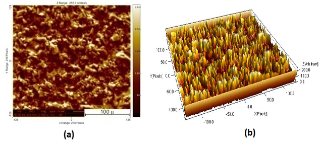
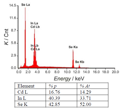
The ternary CdIn2Se4 material was obtained after annealing of the two binary phases, CdSe and In2Se3, under vacuum at 450ºC. Figure 2 shows a scanning electron microscopy (SEM) analysis of the CdIn2Se4 material including a three-dimensional view of the surface coverage and the height distribution of the clusters (obtained using a trial version of the SPIP image processing software).The energy dispersion X-ray (EDX) elemental analysis results for the ternary compound are shown in figure 3.
Crystal Structure
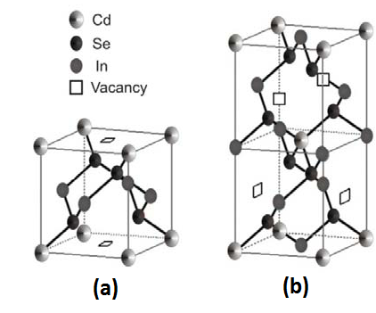
The crystal structure of CdIn2Se4 can be found in three tetragonal poly types, which are referred to as: α, β ,and γ . The α phase is a pseudo-cubic-ordered vacancy structure with space group P (-4) 2m - D12d, as shown in figure 4a. This cell contains one chemical formula; four anions, three captions and therefore, there is one vacant cation site per unit cell with respect to the perfect zinc blende structure. This phase is referred to as 'pseudo cubic' because a = b = c, although the space group is tetragonal. The tetragonal phase β is shown in figure 4b, known as defect chalcopyrite I (-4) 2m. Both phases (β and γ) differ in the c/a = ratio: β: c = 2a, γ: c = 4a.
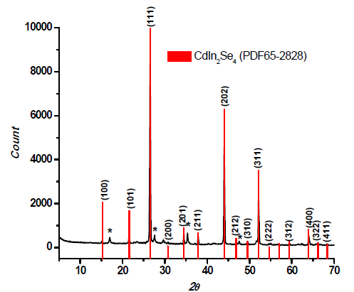
The lattice parameters of the electrochemically deposited material reported in this work were determined by X-ray powder diffraction (XRD) within the (10–70)º 2θ range shown in figure 5.
Further thermal treatment under a selenium atmosphere (at 450°C for 3 h) was found to induce the formation of CdIn2Se4. Figure 5 shows a comparison between the experimental diffraction pattern and the data available at the PDF2 ICDD– 03-065-28-28 data library for CdIn2Se4; they both agree with a crystalline tetragonal structure with preferential (111) orientation.
Optical Absorption Spectroscopy
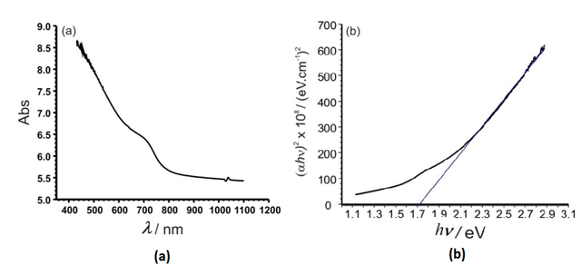
Optical absorption measurements on CdIn2Se4 films were performed at room temperature (25 °C) between 400 and 1100 nm. The results are shown in Figure 6a. Absorption mainly occurs at low wavelength ( λs) values and an absorption border is present. The nature of the transition may be determined from the dependence of the absorption coefficient (α) on hν, which for an allowed direct transition.
The plot of (αhν)2 versus hν in Figure 6b shows the optical transition, the band gap energy value being estimated from the intercept on the x axis (Eg = 1.73 eV); this value is in agreement with previous results reported in the literature.
Electrochemical impedance spectroscopy
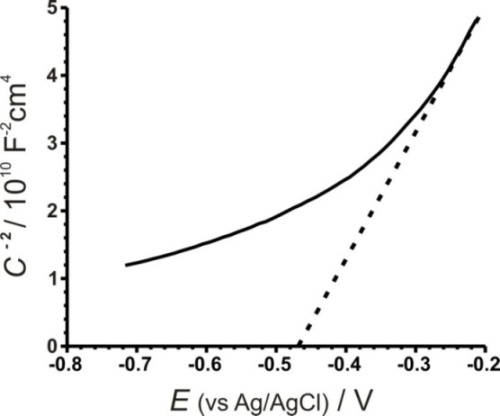
The semiconductor–liquid junction (S–L) of a semiconducting electrode involves the formation of two types of double layers, one at the S–L junction and another one within the space charge region of the semiconductor, giving two types of capacitance. The capacitance due to the S–L double layer is small enough to be neglected so that the measured capacitance can be conveniently considered to be due to the space charge layer. Thus, measurements of the capacitance as a function of the applied bias under depletion conditions provide useful information about the flat band potential, donor density, magnitude of band bending, and width of the depletion layer. The flat band potential, Efb, of a semiconductor gives information about the relative position of the Fermi level in a photo electrode. The measurement of apparent capacitance as a function of potential under depletion conditions is based on the Mott–Schottky relation, as shown in equation 1:
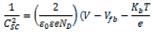
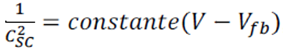
Where Csc is the space charge capacitance per unit area, εe is the electronic charge, is the dielectric constant of the semiconductor, ε0 is the permittivity of free space, ND is the donor density, is the applied voltage, is the Boltzmann constant, and T is the absolute temperature. Since the term (2/ ε0 εe ND) in equation (1) is a constant, by neglecting , equation 1 can be rewritten as:
Impedance measurements were carried out on six different CdIn2Se4 samples at a frequency of 10 kHz. A Mott–Schottky graph for CdIn2Se4 in 1M Na2SO4 (figure 7) allowed us to measure the flat band potential (Efb = -0.468 V). The positive slope of the linear region suggests the presence of major negative carriers and an n-type behavior of the semiconductor (the slope has a value of 19.324). The donor concentration, ND, was calculated from equation 3 and we obtained a value of 7.52E21 cm-3. We assumed that εs was 9.7 for CdIn2Se4 because there is no value available for this semiconductor yet.
The observed linearity deviation in the Mott–Schottky plot suggests that the junctions are of ‘graded type’ and can be attributed to the presence of both shallow and deep donor levels. This behavior is usually observed in polycrystalline films.
To know more about the potential of flat band see the following article "Flat-Band Potential of a Semiconductor: Using the Mott-Schottky Equation"
To complement the information related to the synthesis of this semiconductor I invite you to read the following article "http://citeseerx.ist.psu.edu/viewdoc/download?doi=10.1.1.677.3371&rep=rep1&type=pdf"
Great post. It doesn't seem like you are getting the likes it deserves though. Have you checked out the upvote communities? You should check out steemengine. or steemfollower.com.
thanks, I will review both sites
Congratulations @yan8018! You have completed some achievement on Steemit and have been rewarded with new badge(s) :
Click on any badge to view your own Board of Honor on SteemitBoard.
For more information about SteemitBoard, click here
If you no longer want to receive notifications, reply to this comment with the word
STOP