Are carbon nanotubes the future of manufacturing?
Are carbon nanotubes the future of manufacturing?
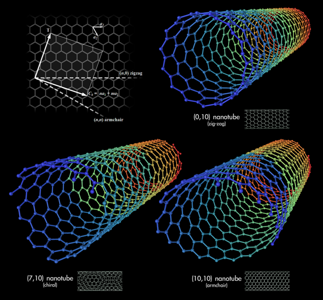
Source
Carbon nanotubes.
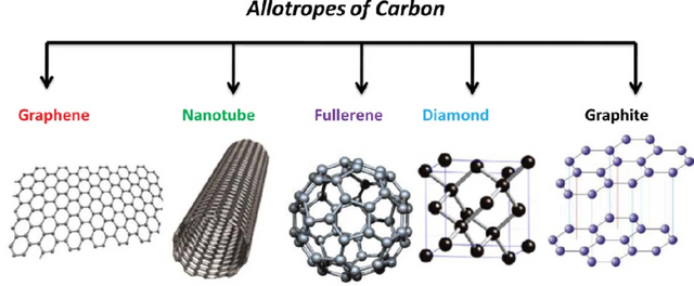
They are basically allotropes of this same element with a cylindrical nanostructure, the allotropy is the property that some chemical elements have to be present under different chemical structures, citing the example of carbon some allotropes of the same are graphite, diamond, graphene, and fullerene.
Due to its structure, nanotubes possess extraordinary characteristics that are very useful for the development of potential applications in various fields of nanoscience and nanotechnology.
Carbon nanotubes were discovered in 1991 by Sumio Iijima, who work on an electron microscope, observed the existence of tubular molecules in the soot formed from electric arc discharges, using graphite. The precursor of the NTC's is fullerene. Fullerenes are an allotropic form of carbon. They were accidentally discovered by the Smalley and Kroto groups in 1985, their discovery was awarded the Nobel Prize in chemistry in 1996. The attempt to produce fullerenes doped with metals resulted in the discovery of the nanotubes, which were initially called Buckytubes. The obtained nanotubes were cylinders closed at the ends by a spherical cap with the structure of a fullerene. These nanotubes presented different structures depending on the orientation of the graphene hexagons with respect to the axis.
Source
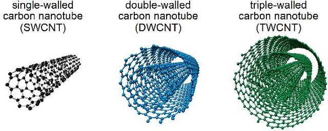
Carbon nanotubes are made up of curved and closed hexagonal carbon networks that form carbon nanometer-sized tubes. We can differentiate between monolayer (single tube) and multilayer (several tubes, one inside the other) nanotubes. These structures are characterized by being light, hollow and porous, with high mechanical resistance, which is why they are of great interest in the structural reinforcement of materials and in the formation of low weight composites.

Source
Types of carbon nanotubes.
Source
Nanotubes Single Wall (SWNT).
A single-walled carbon nanotube can be considered as a cylinder that results from rolling a sheet of graphene on itself. The typical dimensions of it are an atom of thickness, a few tens of atoms of the circumference and some microns in length. Compared with the diameter of the nanotube, the length of the nanotube is much greater, so they are simply considered as if they were elements of a single dimension.
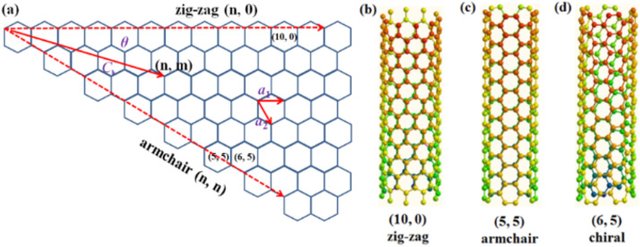
The properties of this class of carbon nanotubes depend mainly on two parameters that are the diameter and the chiral angle. Also called the helicity angle, these two parameters are born the so-called Hamada indexes, which are nothing more than a pair of integers (n, m) that describe the number of unit vectors along the directions a1 and a2.
Source
Most single wall nanotubes (SWNT) have a diameter of about 1 nanometer and can be many millions of times longer. The structure of a SWNT can be conceptualized as the wrapping of a graphite layer an atom of graphite thickness called graphene, in a transparent cylinder. The way to wrap the graphene sheet is represented by a pair of indexes (n, m). The integers n and m indicate the number of unit vectors along two directions in the crystalline lattice honeycomb of graphene. If m = 0, the nanotubes are called zigzag nano-tubes, and if n = m, the nanotubes are called armchair nanotubes. If it's the other way around, they're called chiral.
Source
Multiple wall nanotubes (MWNT).
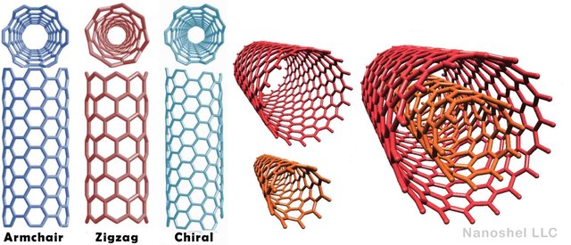
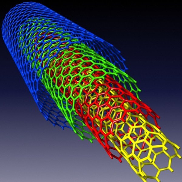
Multiple wall nanotubes (MWNT) consist of several laminated layers (concentric tubes) of graphene. There are two models that can be used to describe the structures of multi-walled nanotubes. In the Russian doll model, the graphite sheets are arranged in concentric cylinders, for example, a nanotube (0.8) of a single wall (SWNT) inside a larger nanotube (0.17) of a single wall. In the Parchment model, a single sheet of graphite is wound around itself, resembling a roll of parchment or a rolled newspaper. The distance between layers of multiple wall nanotubes is close to the distance between the graphene layers in the graphite, approximately 3.4.
Double-walled carbon nanotubes (DWNTs) form a special class of nanotubes since their morphology and properties are similar to those of SWNT, but their resistance to chemicals is significantly improved.
Source
Applications of Nanotubes.
Due to the extraordinary characteristics of the nanotubes they have applications in a myriad of fields, below are the most interesting ones and those that promise a greater technological development:
- Flexible Supercapacitors.
Supercapacitors are traditionally defined as capacitors that have a capacity two or three times greater than that of a common capacitor. In the capacitors formed by nanotubes, the latter is deposited in arrays forming a kind of matrix, with this, it is possible to generate two electrodes between which a dielectric is placed, see figure 6. Recent studies have shown that the response of the capacitors improves to 30% when using capacitors based on nanotubes.
- Materials with exceptional physical properties.
In many fields, nanotubes have already been used to improve the mechanical properties of materials by adding a small fraction of nanotubes in their composition, for example, several parts of bicycles, sailboats and even compounds have been created that are activated providing greater hardness. It has been proposed that nanotubes be used as a structural raw material for the construction of a possible space elevator because they would be the only materials that could withstand the enormous fatigue to which the device is exposed in space, due to the gravity and rotation land.
- Fuel Storage.
The nanotubes are capable of absorbing any gas due to the capillary effect that they possess, which is why they have been considered to be used in the storage of hydrogen-based fuels. [4,16]. A great disadvantage is that the absorption of hydrogen in the nanotubes only occurs in a controlled environment, at a certain temperature and by stimulation of an electric current, however, currently there are great advances that already allow absorption at room temperature.
- Electric field emission microdevices.
Due to the properties of being able to be metals or semiconductors, nanotubes have been used as small electric field emission devices, through which they have been able to create extremely small transistors. This has enabled the development of small screens with nanotubes as a means of emitting the electrons needed to activate light-emitting diodes and thus produce the image.
- Biochemistry and Biosensors.
The electronic and structural properties of carbon nanotubes make them very attractive for bio-electromechanical applications, and some electrons have been shown to be able to improve the synthesis of enzymes and other proteins, but this is still a very experimental one due to the fact that nanotubes by adhering completely to the solution in which they are diluted, they hinder the communication of the enzymes.
In electronics.
The current trend is the miniaturization of devices to improve performance: speed increase, density and efficiency, and it is due to these circumstances that these materials seem to have a great future within the electronics at the mesoscopic scale. Another property of noteworthy carbon nanotubes, important in the world of electronics, is that they are excellent conductors of heat, which makes them perfect heat dissipators that occurs in electronic systems
Conclusions.
It has been observed that nanotubes have unique characteristics, both in their physical structure and in their electronic configuration, for this reason, they have an almost unlimited number of applications, being possible to use them in all the fields either to produce new materials and devices or to improve the physical properties of a material in question.
However, there are also many limitations, especially in large-scale production methods and the determination of certain characteristics of these materials, which still require studies and the development of new technologies to improve understanding of this revolutionary technology.
As a final point, a factor to take into account would be the economic change that would produce the development of materials based on nanotubes since on the one hand, it would improve the production and sales of certain companies by offering a higher quality product.
Reference:
- http://www.nanoscience.com/applications/education/overview/cnt-technology-overview/
- https://www.sciencedaily.com/terms/carbon_nanotube.htm
- http://science.sciencemag.org/content/339/6119/535.full
- Handbook of Environmental Degradation of Materials, Myer Kutz
- Carbon nanotubes, Silvana Fiorito

These will have neat applications in material science. One such is increasing interlayer adhesion in 3d prints.
Yes, the new 3d nanomaterials are the future, I invite you to read a post related to that
https://steemit.com/steemstem/@giovaabbatichio/is-this-the-new-way-to-generate-energy
Great article ! definitely deserves an upvote !
thanks!
interesting research
thanks
You could build an entire super structure in space using 3d printed nanotubes.
Definitely the uses of nanotubes is almost infinite
Congratulations! This post has been upvoted from the communal account, @minnowsupport, by giovaabbatichio from the Minnow Support Project. It's a witness project run by aggroed, ausbitbank, teamsteem, theprophet0, someguy123, neoxian, followbtcnews, and netuoso. The goal is to help Steemit grow by supporting Minnows. Please find us at the Peace, Abundance, and Liberty Network (PALnet) Discord Channel. It's a completely public and open space to all members of the Steemit community who voluntarily choose to be there.
If you would like to delegate to the Minnow Support Project you can do so by clicking on the following links: 50SP, 100SP, 250SP, 500SP, 1000SP, 5000SP.
Be sure to leave at least 50SP undelegated on your account.
I like your post...nanotechnology is the future!
Yes, it is. I think nanotechnology is going to change the world