Seeing the electricity inside graphene for the first time
In the race towards faster and smarter next-generation electronics, including quantum computers, researchers at the University of Melbourne are the first in the world to image how electrons move in two-dimensional graphene.
Made up of a lattice of carbon atoms only one atom thick, graphene is a key material for the electronics of the future. The ultimately thin carbon material is stronger than steel and due to its flexibility, transparency and ability to conduct electricity, holds great promise for use in solar cells, touch panels and flexible electronics.
Now a team led by Professor Lloyd Hollenberg, Deputy Director of the Centre for Quantum Computation and Communication Technology (CQC2T), has used a special quantum probe based on an atomic-sized ‘colour centre’ found only in diamonds to “see” the flow of electric currents in graphene for the first time.

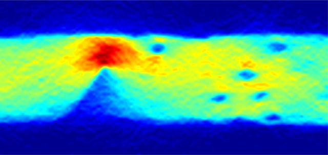
Image of the electron flow from gold leads to graphene obtained with the diamond quantum sensor, revealing imperfect contacts. Picture: University of Melbourne/cqc2t.org
No one has previously been able to see what is happening with electronic currents in graphene says Professor Hollenberg, who holds the Thomas Baker Chair at the University of Melbourne.
According to Professor Hollenberg, this new technique overcomes significant limitations with existing methods for understanding electric currents in devices based on ultra-thin materials.
“The ability to see how electric currents are affected by these imperfections will allow researchers to improve the reliability and performance of existing and emerging technologies,” Professor Hollenberg says. “We are very excited by this result, which brings quantum probe-based imaging to the world of graphene nanoelectronics and quantum computers.”
Quantum computers will harness the power of atoms and molecules to perform memory and processing tasks, and have the potential to perform certain calculations significantly faster than any conventional computer.
But next-generation electronic devices based on ultra-thin materials, including quantum computers, will be especially vulnerable to contain minute cracks and defects that disrupt current flow.
The success of the new sensing technique means researchers now have the potential to observe how electrons move in such tiny structures.
“These observations could aid our future understanding of how quantum computers will operate, as well as contribute to our understanding of electron behaviour in new and emerging technologies,” Professor Hollenberg says.
Lead author Dr Jean-Philippe Tetienne, from CQC2T at the University of Melbourne, explains how the team was able to use diamond to successfully image the current.
“Our method is to shine a green laser on the diamond, and see red light arising from the colour centre’s response to an electron’s magnetic field,” he says.

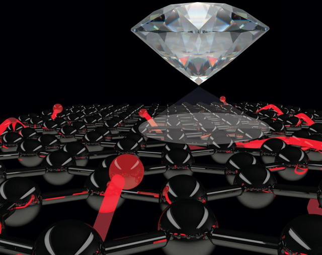
Artist’s impression of a diamond quantum sensor. The ‘spotlight’ represents light passing through the diamond defect and detecting the movement of electrons. Electrons are shown as red spheres, trailed by red threads that reveal their path through graphene (a single layer of carbon atoms). Picture: David A. Broadway/cqc2t.org
“By analysing the intensity of the red light, we determine the magnetic field created by the electric current and are able to image it, and literally see the effect of material imperfections.”
Researchers at CQC2T have led the world in atomic-scale fabrication of nano-electronics in silicon for quantum computers. Like graphene sheets, these nano-electronic structures are essentially only one atom thick.
“Our technique is powerful yet relatively simple to implement, which means it could be adopted by researchers and engineers from a wide range of disciplines,” says Dr Tetienne.
“Using the magnetic field of moving electrons is an old idea in physics, but this is a novel implementation at the microscale with 21st century applications.”
The work is a unique collaboration between diamond-based quantum sensing and graphene researchers. Their complementary expertise was crucial to overcoming technical issues with combining diamond and graphene.
“Building a device that combined graphene with the extremely sensitive nitrogen vacancy colour centre in diamond was challenging, but an important advantage of our approach is that it’s non-invasive and robust – we don’t disrupt the current by sensing it in this way”, said Nikolai Dontschuk, a graphene researcher at the University of Melbourne School of Physics.
The current-imaging results have been published in the prestigious Science Advances journal and are the culmination of a year’s work. The research is supported with funding from the Australian Research Council through the Centre of Excellence and Laureate Fellowship programs.
Banner image: Artist’s impression of the experimental setup for a quantum sensing experiment. The diamond quantum sensor is controlled by lasers. An atomistic representation of graphene (a single layer of carbon atoms) sits atop the sensor. Red lines represent the trajectory of the electrons as they move through the graphene. David A. Broadway/cqc2t.org
Original article: http://blogs.unimelb.edu.au/quantum-technology/publications/
Congratulations @parax14! You received a personal award!
Click here to view your Board
Do not miss the last post from @steemitboard:
Congratulations @parax14! You received a personal award!
You can view your badges on your Steem Board and compare to others on the Steem Ranking
Do not miss the last post from @steemitboard:
Vote for @Steemitboard as a witness to get one more award and increased upvotes!