Introduction to electronics
Electronics is a branch of science, technic and technology that studies movement of electrically charged particles through vacuum, gas and semiconductors and based on that study it engages in design and construction of electronic devices.
Basic electronic devices are electronic elements with characteristics suitable for performing basic electronic functions, e.g. signal amplification or aliasing. Basic electronic functions are done by electronic circuits. Those are simple networks built by interconnecting electronic elements with other electronic elements like resistors, capacitors and inductors. Connecting a larger number of electronic circuits, electronic systems are formed. They are designed to perform complex electronic functions in controlling, processing and distribution of information, and in transformation and distribution of electrical energy.
Development of electronics
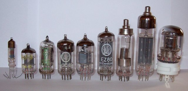
The beginning of classical electronics was in first period of 20th century when the first electronic elements were invented - vacuum tubes.
Those were vacuum diode (Fleming - 1904.) and triode (de Forest - 1906.). The first elements were working based on movement of electronics emitted from the incandescent electrode. Electrons moved in vacuum inside the tube under the influence of electrical field.
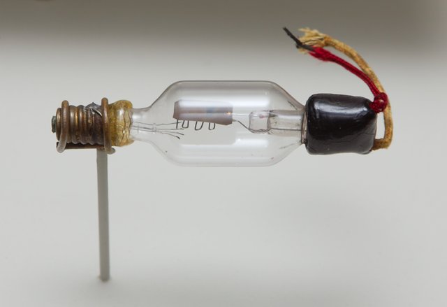
And while vacuum diode, an element with 2 electrodes, was characterized by corrector properties, i.e. good electricity conduction on one voltage polarity and outage on the opposite polarity, in triode, amplification of the signal was enabled by introducing the third electrode.
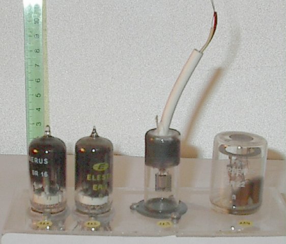
Along with the diode and triode, advanced vacuum tubes with larger number of electrodes and gas filled tubes were used. Using the basic, tubular circuits complex circuits were designed (electronic system) like radio and TV receivers, transmitters, radars, analog computers and similar.
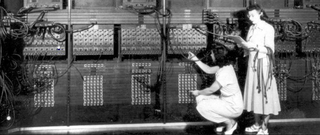
Using the vacuum tubes, first digital electronic computer was built (ENIAC - 1946.) and it consisted of 18.000 tubes and occupied an area of 10x13 meters. (Fun fact: first programmer was a women :) )
Although they were quality electronic elements, electronic tubes had significant deficiencies like relatively big dimensions, great power consumption and limited period of duration of its filament. That's why in the first half of 20th century, further research in development of semiconductor elements has started.
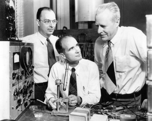
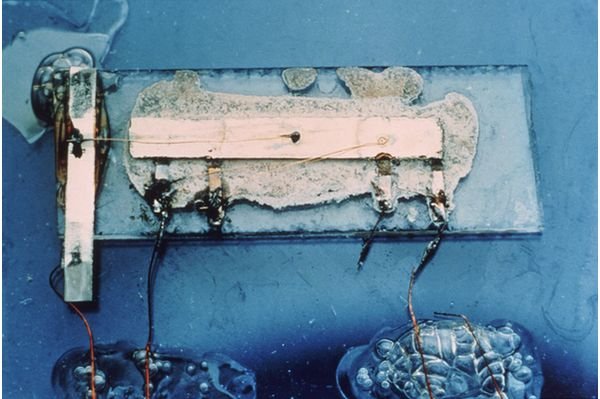
The real beginning of modern semiconductor electronic is related to the invention of bipolar transistor (Brattain, Bardeen - 1948.). That was a dotted germanium transistor with the signal amplification property. Along with the construction of first semiconductor elements, Shockley has developed theory of their work. Based on his research, already in 1951. dotted bipolar transistor with bad characteristics was replaced by junction field-effect transistor.
![]()
Thanks to its properties (significantly smaller dimensions, lesser power consumption, greater reliability) semiconductor elements were rapidly replacing electronic tubes in practically all electronic applications except in the area of high voltages and power.
![]()
Main drawback of semiconductor elements were the temperature changes of their characteristics. Because of that deficiency, starting semiconductor material germanium (Ge), whose elements worked on temperatures up to around 75° C, in the end of 50's was already more and more replaced by silicon (Si) which enables elements to perform up to around 200° C.
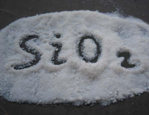
Along with the better temperature properties, important characteristic of silicon was easy oxidation of its surface, wherein a layer of silicon dioxide (SiO2) was formed. Silicon dioxide as a dielectric was a part of the MOS transistor structure, whose wider use starts 1960.
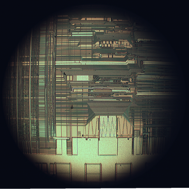
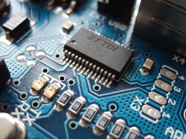
Using the silicon dioxide a planar production technology of silicon semiconductor structures was developed. Except for the production of quality discrete semiconductor elements, planar technology has also started a new era of electronics - an era of integrated circuits. Integrated circuit is a structure in which all circuit elements are realized on the same semiconductor tile (transistors, diodes but also resistors and capacitors) and interconnected in a functional whole.
Although the first generation of individual semiconductor elements connected in the same casing was accomplished in germanium technology (Kilby - 1958), first integrated circuit on the silicon board was realized using the planar technology (Noyce 1959.).
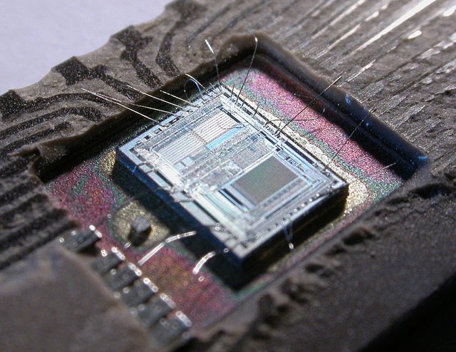
Integrated circuits have soon started replacing the electronic circuits built using the discrete elements. Advantages of integrated circuits are small dimensions, low power consumption, greater reliability and cheap price. First integrated circuits have consisted of around 10 elements. Sudden development of the semiconductor technology enabled reducing the minimum dimension of single element on the circuit, and therefore integration of increasing number of elements on one silicon board - a chip.
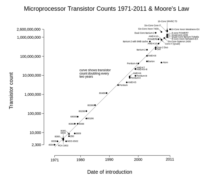
Already in 1964. Moore predicted that the number of the components will double every 18 months (Moore's law). His predictions have been held to date. Complexity of the chip was rising as number of basic elements on the board was increasing. Except for the basic electronic circuits, soon the complex electronic system were also being integrated on the same silicon board.
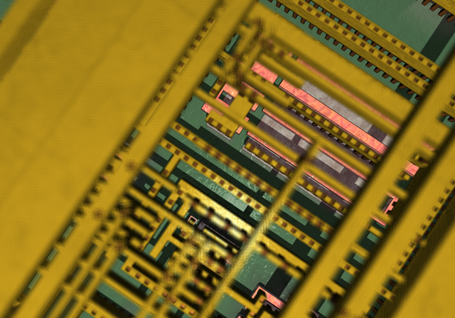
Today's technology enables integration of as many as 2^31 elements on the chip. Using that number of elements results in integration of highly complex electronic systems like microprocessors or semiconductor memories of great capacities, which are the foundations of IT industry. Although the first integrated circuits were founded on the application of bipolar transistors, as early as in 70's, especially in the digital electronic, the simpler MOS transistors became prevalent.
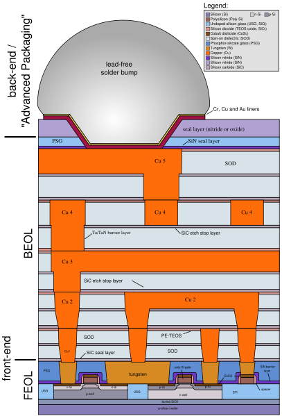
Big part of today's integrated circuits are CMOS circuits, i.e. circuits based on the application of complementary MOS transistors.
Parallely to the expansion of silicon integrated circuits of great complexity have been developed electronic elements and circuits of specific properties and applications. In the areas of high speed performances there have been developed elements and integrated circuits in technology of gallium-arsenide (GaAs). Their use is significant in the area of mobile communications.
Special group of elements is formed by optoelectronic elements which are used for transformation of light energy to electrical energy and vice versa. In that area there have been developed elements like solar cells, photodiodes, phototransistors, light diodes, semiconducting lasers etc. In the design of optoelectronic elements many different semiconductor materials are used.
Summary
In the realization of electronic circuits and system, primarily are used semiconducting electronic elements whose work is based on the current flowing through the semiconductor. Semiconductors are a group of materials with specific conductivity lesser than specific conductivity of conductors and greater than specific conductivity of isolators. Basic property of semiconductor, which laid foundation for their widespread use in electronics, is the possibility to adjust specific conductivity in wide limits, whether through the change of composition of materials, or using the outer influences.
In other words, semiconductors are founding blocks of transistors, which are a programmable resistors/amplifiers. You can imagine it like a little switch you can turn on and off on using a signal. So simple yet so revolutionary. The transistor is the key active component in practically all modern electronics. Many consider it to be one of the greatest inventions of the 20th century.

Properties of solids are defined by the arrangement of atoms or groups of atoms. With the regular arrangement of atoms the material is a crystal, and if arrangement irregular we are talking about amorphous material. Crystal materials can be either monocrystalline, with regular arrangement of atoms in the whole volume or polycrystalline, which consist of large number of monocrystalline grains. Regularity of the arrangement of atoms inside a grain is broken on the brain borders.
![]()
In the next post I will talk about the monocrystalline materials with well defined electrical properties as they are most interesting for electronics.
Thank you for reading.
Dear @eneismijmich,
Your post has been selected by the @robinhoodwhale initiative as one of our top picks for curation today.
Learn more about the Robinhood Whale here!
The Steemit community looks forward to more amazing blogs from you. So, please keep on Steeming!
Goodluck!
~RHW~
Vote my post too please. I'm poor as beggar :( I'm trying my best to give good post..
This led to microprocessors, personal computers, internet and blockchain among many other things.
Thanks for your post! This recalls me my visit of the computer history museum at Palo Alto in California where you can follow the 2000 years of computer history ;)
WTF! This is an awesome post! Thanks.
Very informative post!
Nice research @eneismijmich!