Semiconductors and P-N Junction Diodes
Introduction
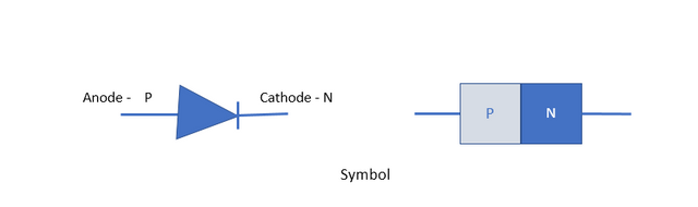
Have you ever heard the word "Diode"? A Diode is an electronic component which is basically used as a switch and has two electrodes called anode and the cathode. Most diodes are made with semiconductor materials such as silicon, germanium. There are various kinds of diodes, but we'll concentrate on P-N Junction Diode.
What are Semiconductors you ask?
A semiconductor material is a material which has an electronic conductive property that falls between that of conductive materials (copper, gold, etc) and insulators (such as glass, wood, etc)
the semiconductor only allows the currents to flow in specific conditions such as very low temperatures and also adding impurities to the material.
Symbol and notation
The diodes allow current to flow through it in one direction with greater ease way than in the other device. acting as a switch depending upon the direction of the current. Below are the symbols for the diodes used in the schematic diagrams for circuits.
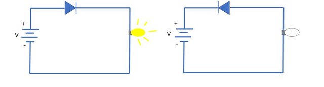
Example circuit
for example when a diode is placed in a single battery-bulb circuit (picture below), then the diode will either allow or block the current through the bulb, depending on the polarity of the applied voltage.
Diode Operation
when the Current flow is permitted, the diode is called in forward biased. and when the Current flow is prohibited, the diode is reversed biased.
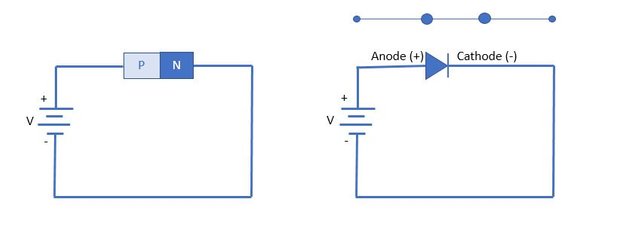
Biasing
Method of applying the necessary voltage across P-N Junction (P stands for positive and N stands for negative, Duh!!) is known as Biasing. There are two methods of biasing.
Forward Bias
In forward bias, the anode is connected to positive terminal of the supply and cathode is connected to negative terminal of the battery supply.
what happens when we connect Forward Bias? here's what happens.
In forward bias electrons in N-region get repelled from the negative terminal of the battery and they enter into P-region.
At the same time, electrons enter into N-region from the negative terminal of the battery.
In this way a continuous current flow through a diode when it is forward biased.
Here it acts as a closed switch.
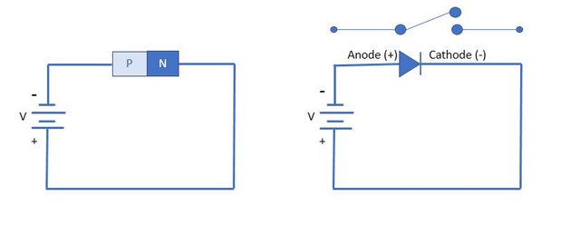
Reverse Bias
When P- region(anode) is connected to negative terminal & N-region(cathode) is connected to positive terminal, diode gets reverse biased.
In this case the 'holes' & 'electrons' move away from the junction.
There are very few electrons in P-region, which enter from N-region, therefore very small leakage current flows.
This current is called reverse leakage current.
There is a limitation to the maximum forward & reverse voltage that can be applied to the diode.
When a large reverse voltage is applied across the diode, heavy current flows through it.
This is called as break down of diode & The voltage at which diode breaks down is called as break down voltage.
If the reverse voltage is further increased, the diode may get damaged permanently.
The maximum reverse voltage that can be applied to the diode without damaging is called Peak Inverse Voltage (PIV).
What did a diode in the reverse biased state said to the electrons?
Created using imgflip.com

P-N Junction
Now we will discuss P-N Junction and the formation of the depletion layer.
Depletion Layer
The n-type semiconductor in which pentavalent impurity mixes, An extra electron remain and by Poly Exclusion Principal every electron of pentavalent be a free electron.
In P-type semiconductor trivalent impurity mixes, Every trivalent atom has the power to accept an electron.
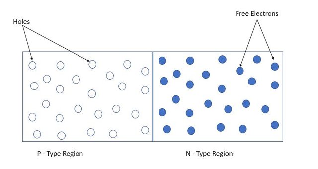
There is a boundary between P-type and N-type region. In the P-type region, Holes are present and in N-type region free electrons are present. These free electrons propagate and fill the holes in P- region.
In N-type region, these free electrons are neutral before moving. As soon as these electrons move to holes, This region becomes a positive charge region.
When free electrons fill the holes in the P-type region, This P-region get a negative charge so here some negative charge resides.
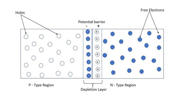
at last, there'd be a region, In which there's no charge carrier, as well as in this region one side get the net positive charge and other side gets a net negative charge. This region is called the Depletion Layer. In Forward-bias the layer gets thinner and in Reverse-bias it gets wider.
Voltage & Current Characterstics Of a P-N Junction
Now we will see the relation between voltage & current with the P-N Junction. we will also see how if the P-N Junction is in forward-bias then whats the relation of voltage and current. If there is reverse bias then whats the relation between voltage and current.
- In forward-bias the free electrons propagate to the holes and fill the holes at the boundary in the P-type region then there is no more charge carrier at the boundary of N-type region and P-region and this region called depletion layer.
- When it is connected in forward-bias that means negative terminal connected to the N-side and the positive terminal of the battery is connected to the P-side From this negative terminal push the electron and in P-region which is higher potential side will attract the electron and fill the hole. These electrons propagate through the holes and all electrons will propagate the same way, due to which the depletion layer remain thin now a very little amount of current will flow.
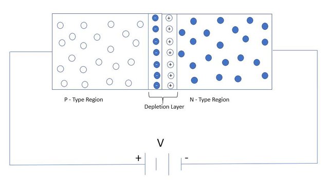
Here the electron moves from the negative terminal to the positive terminal that means the current is flowing. when we increase the voltage then the more current will flow.
At the certain point (a) this potential barrier will totally disappear and here Depletion layer also disappear and all the electron which capture the holes will also move, As well as these free electrons will fill the depletion layer because there is no potential barrier and there is no region to resist it now current will flow efficiently with more voltage.
Now this acts as a conductor and we get to the point (a) there is no potential barrier on this stage. So it will react as a conductor and this voltage called knee voltage and the value of the knee voltages are as below
       0.3v For Germanium
       0.7v For silicon
Now see what happened when P-N Junction connected in the reverse bias.
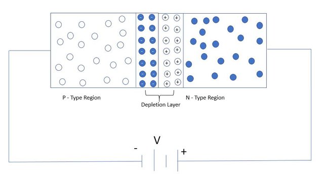
In the reverse bias negative terminal connected to the P side and positive terminal connected to the N side. In this process, negative terminal push the electrons and these electrons fill the holes and this will attract some electron from the positive side and in N-side electron will move that means some current will flow.
This current varies with voltage slowly and it has very low magnitude. This flow very low current.
These are the Characteristic of voltage and current for P-N Junction below.
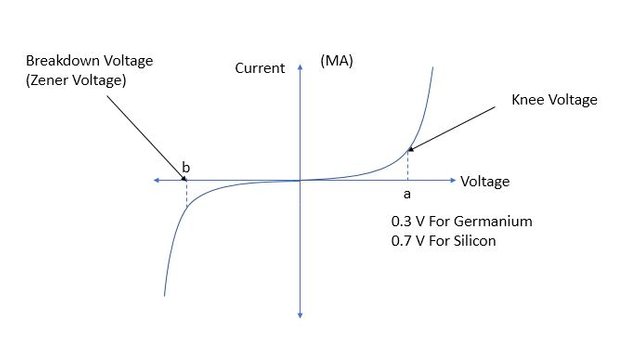
Here if we increase the voltage then it resists the current so the current increase very slowly and if we increase the voltage continuously then at the certain point (b) this will show the breakdown of the P-N junction and this breakdown is called Avalanche breakdown.
After this point, it will out of order. When voltage increase again, The magnitude of the current will highly increase.This point (b) is also known as Zener voltage.
Applications
Diodes are used for various purposes, some of the applications are listed below.
- Diodes are used as a switch in circuits.
- Used in rectifiers which converts AC Current to DC Current.
- Used in Clipper and Clamper Circuits.
- also you probably know LED, which stands for "Light Emitting Diode."
References: A Lecture on Basic Engineering Electronics by Ms. Leena Taiwade, A textbook called "Fundamentals of Electrical Engineering and Electronics" by B L Theraja, all the images in the post are self-created unless stated otherwise.


gif Created by @foundation
Daily Fun Fact #60 -- "Silicon makes up 27.2% of the Earth's crust by weight, second only to oxygen at 45.5%."
More Information
Brings back my School Physics memories.
It's a good thing, right?
This post has received a 1.96 % upvote from @drotto thanks to: @arrjey.
you are scaring me man!
lol, sorry, didn't mean to scare. :P
This post has received a 3.85 % upvote from @steemdiffuser thanks to: @arrjey. Steem on my friend!
Above average bids may get additional upvotes from our trail members!
Get Upvotes, Join Our Trail, or Delegate Some SP
omg nerd