LED BLINKING USING PIC CONTROLLER
Today we are going to write code from scratch. But how to write the code for PIC controller? So before starting to writing, the code we need MPLAB X IDE v4.00 compiler. This compiler is simple and easy to use. I will show step by step process of MPLABX IDE V4.00.
You can Download and Install MPLAB X IDE v4.40 and MPLAB XC8 Compiler. Here we are going to use PIC18F452 controller for LED blinking.
So let's start.......
HOW TO USE MPLABX IDE v4.40?
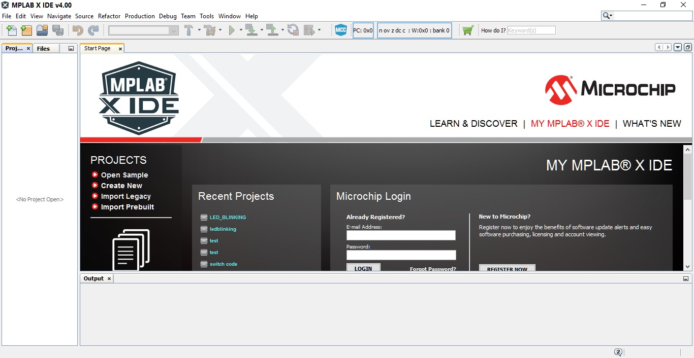
Step1:- Double click on the icon of MPLAB X IDE v4.00. The MPLAB X IDE welcome window will appear.
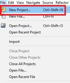
Step2:- Now go to FILE->NEW PROJECT.
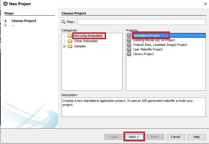
You will see NEW PROJECT screen.
Step3:- Click on MICRO-CHIP for Categories and STANDALONE PROJECT for Projects. Now click NEXT.
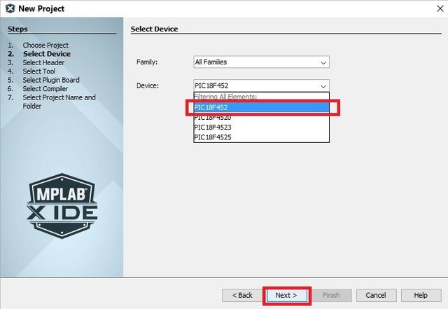
Step4:- Now you have to select device. In our case we are going to use PIC18F452 controller. Just select PIC18F452 from Device dropdown and click NEXT.
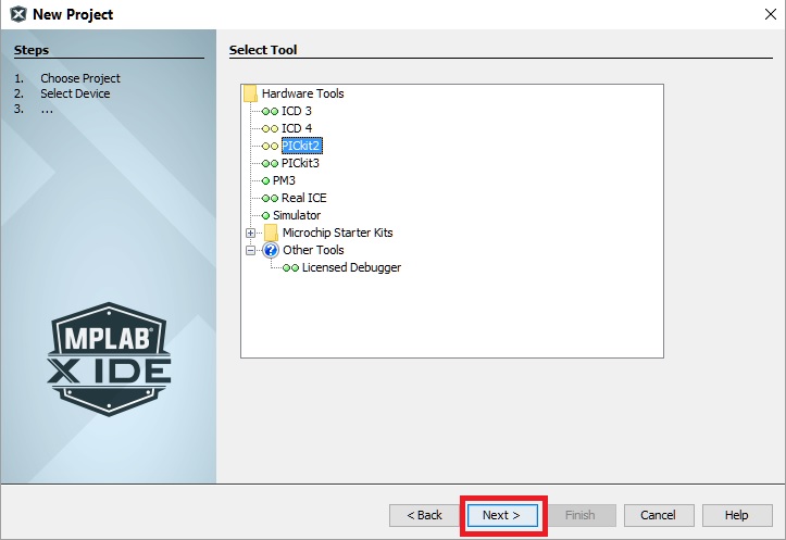
Step5:- Here we have to select programmer which will help us to load HEX code into the controller. In SELECT TOOL section I am going to use PICkit2. If you don’t have PICkit2 you can select Simulator. Now simply click NEXT.
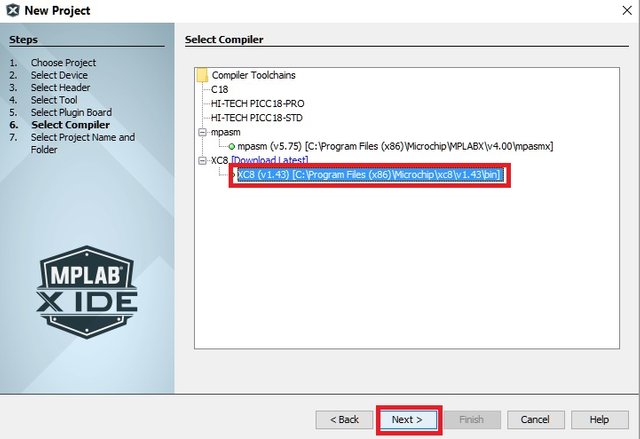
Step6:- In Select compiler section, we are going to use XC8 (v1.43) compiler. Click NEXT.
Step7:- In Select project Name and Folder section, we have to create folder where our project is going to save.
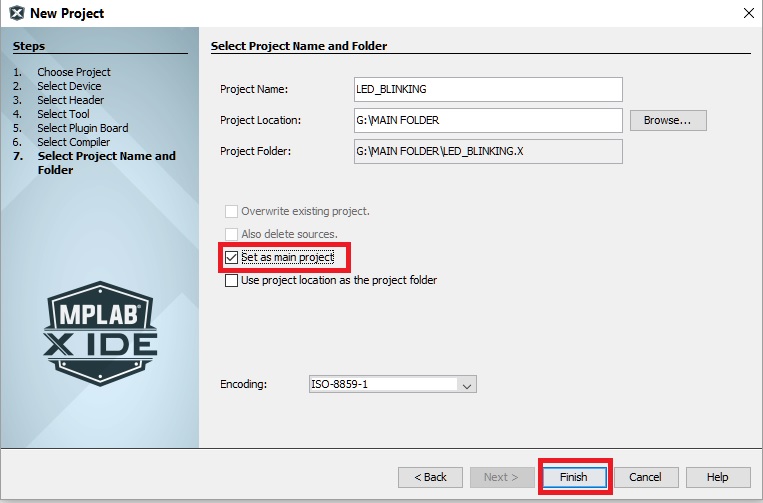
Before writing name in “Project Name” section, go to “Project Location”. Browse the location where you are going to save the file. After that give the “Project Name”. Click on finish button.
Step8:- Now on left hand side you will see project name “LED_BLINKING” in projects windows. Click on plus sign of LED_BLINKING.

Step9:- Go to “Source File”->> Select it. Now right click on mouse a tab will appear, go to
NEW->> “C MAIN FILE” CLICK.
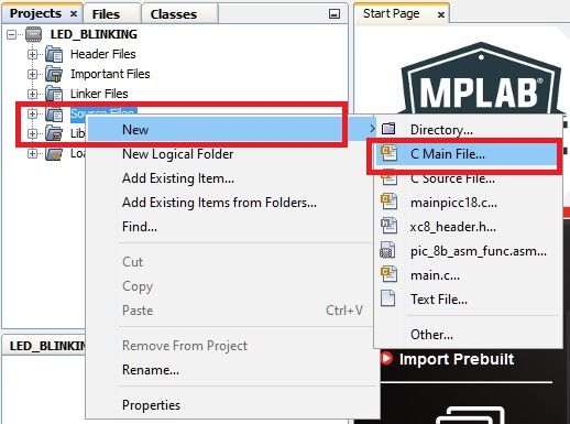
Step10:- Now on your screen new window will appear “NEW C MAIN FILE”. Here type the name of your project “LEDBLINKING” in File Name. EXTENTION SHOULD BE “C” .NOW CLICK FINISH.
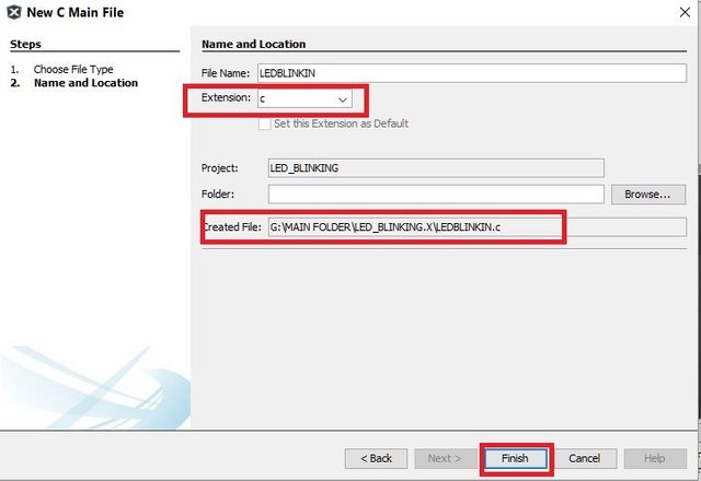
Step11:- FINALLY you will see window. We going to write code within these RED BOX.
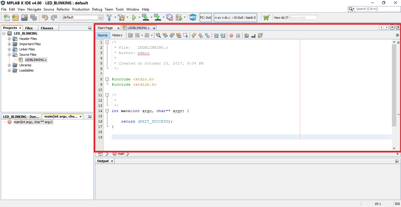
Step12:- Once you finish writing code, now it’s time to “BUILD” the code. Click on icon shown below.

Now you must have understand how to use the MPLAB X IDE v4.00. So now we are going to see programing part how to blink LED using Pic controller. Here we are going to understand “TRIS” and “PORT”.
**Why we need TRIS Register OR PORT?
The answer is simple when we give the power to the PIC controller or after reset, all Port became inputs. So this is done to avoid driving an output pin directly to the VDD or VSS To define the type of an I/O pin, you use the TRIS register. **
TRIS (DIRECTION CONTROL REGISTER):-
TRIS is an 8-bit register, when we set BIT 0 it’s corresponding to pin 0. Let’s see the example below:-
** 7 6 5 4 3 2 1 0 **
0 0 0 0 0 0 0 1
    **WHEN,**   1 = INPUT
                         0 = OUTPUT
Here we see Bit 0 is set ‘1’ it means the direction of these particular pin will became input. An remaining pin is now acting or functioning as output as its set as ‘0’. We can also set all 8 bit by simply assigning ‘1’ or ‘0’ in decimal foam.
Example: - TRISB = 1; // Direction of the Port B is acting as an input.
TRISB= 0; // Direction of the Port B is acting as an output.
PORT REGISTER:-
Now it’s time to control the pin by simply assigning or checking the status of the particular pin wheatear it’s high or low. When the controller sense high or low signal it will perform the task as per the given code. When PORT X is high means voltage of that particular pin is +5 Volts. When PORT X is low means voltage of particular pin is 0 Volt.
**PROGRAM:-
#define _XTAL_FREQ 12000000 //12MHz crystal is used
#include <xc.h>
// PIC18F452 Configuration Bit Settings
// 'C' source line config statements
// CONFIG1H
#pragma config OSC = HS // Oscillator Selection bits (HS oscillator)
#pragma config OSCS = OFF // Oscillator System Clock Switch Enable bit (Oscillator system clock switch option is disabled (main oscillator is source))
// CONFIG2L
#pragma config PWRT = OFF // Power-up Timer Enable bit (PWRT disabled)
#pragma config BOR = ON // Brown-out Reset Enable bit (Brown-out Reset enabled)
#pragma config BORV = 45 // Brown-out Reset Voltage bits (VBOR set to 4.5V)
// CONFIG2H
#pragma config WDT = ON // Watchdog Timer Enable bit (WDT enabled)
#pragma config WDTPS = 128 // Watchdog Timer Postscale Select bits (1:128)
// CONFIG3H
#pragma config CCP2MUX = ON // CCP2 Mux bit (CCP2 input/output is multiplexed with RC1)
// CONFIG4L
#pragma config STVR = ON // Stack Full/Underflow Reset Enable bit (Stack Full/Underflow will cause RESET)
#pragma config LVP = OFF // Low Voltage ICSP Enable bit (Low Voltage ICSP disabled)
// CONFIG5L
#pragma config CP0 = OFF // Code Protection bit (Block 0 (000200-001FFFh) not code protected)
#pragma config CP1 = OFF // Code Protection bit (Block 1 (002000-003FFFh) not code protected)
#pragma config CP2 = OFF // Code Protection bit (Block 2 (004000-005FFFh) not code protected)
#pragma config CP3 = OFF // Code Protection bit (Block 3 (006000-007FFFh) not code protected)
// CONFIG5H
#pragma config CPB = OFF // Boot Block Code Protection bit (Boot Block (000000-0001FFh) not code protected)
#pragma config CPD = OFF // Data EEPROM Code Protection bit (Data EEPROM not code protected)
// CONFIG6L
#pragma config WRT0 = OFF // Write Protection bit (Block 0 (000200-001FFFh) not write protected)
#pragma config WRT1 = OFF // Write Protection bit (Block 1 (002000-003FFFh) not write protected)
#pragma config WRT2 = OFF // Write Protection bit (Block 2 (004000-005FFFh) not write protected)
#pragma config WRT3 = OFF // Write Protection bit (Block 3 (006000-007FFFh) not write protected)
// CONFIG6H
#pragma config WRTC = OFF // Configuration Register Write Protection bit (Configuration registers (300000-3000FFh) not write protected)
#pragma config WRTB = OFF // Boot Block Write Protection bit (Boot Block (000000-0001FFh) not write protected)
#pragma config WRTD = OFF // Data EEPROM Write Protection bit (Data EEPROM not write protected)
// CONFIG7L
#pragma config EBTR0 = OFF // Table Read Protection bit (Block 0 (000200-001FFFh) not protected from Table Reads executed in other blocks)
#pragma config EBTR1 = OFF // Table Read Protection bit (Block 1 (002000-003FFFh) not protected from Table Reads executed in other blocks)
#pragma config EBTR2 = OFF // Table Read Protection bit (Block 2 (004000-005FFFh) not protected from Table Reads executed in other blocks)
#pragma config EBTR3 = OFF // Table Read Protection bit (Block 3 (006000-007FFFh) not protected from Table Reads executed in other blocks)
// CONFIG7H
#pragma config EBTRB = OFF // Boot Block Table Read Protection bit (Boot Block (000000-0001FFh) not protected from Table Reads executed in other blocks)
// #pragma config statements should precede project file includes.
// Use project enums instead of #define for ON and OFF.
int main()
{
TRISB0 = 0; //RB0 as Output PIN
while(1)
{
TRISBbits.TRISB0 = 1; // LED ON
__delay_ms(1000); // 1 Second Delay
TRISBbits.TRISB0 = 0; // LED OFF
__delay_ms(1000); // 1 Second Delay
}
return 0;
}
**
In program #define _XTAL_FREQ 12000000 is given to defines the clock frequency of the microcontroller in program it’s used to calculate delay in __delay_ms() function.
After that we have used #include <xc.h> includes the header file xc.h which contains the definition of __delay_ms() function and TRIS, PORT registers.
Now we will see How to set configuration bits.
Step1:- Go to WINDOW -> PIC MENMORY VIEWER -> CONFRIGURATION BITS -> CLICK ON IT.
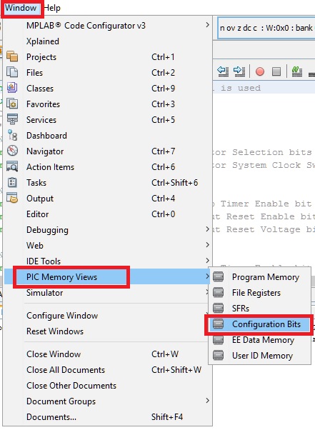
Step2:- You will see configuration bits window at bottom. Set the configuration bit as per your requirement. After that click on GENTRATE CODE.

Step3:- After clicking Generate Code you will see, Config Bit source window. Now just copy the code and past it in your program.

Now write code and compile it.